NEET UG · Video

Diode as Rectifier NEET Concepts
Learn rectifier applications with circuits & MCQs.
6 min video

NEET UG · Physics
Revise the concepts. Try a question. Understand your next step.
13 easy questions available · Try answers free. Sign in to save progress or take a quiz.
NEET UG · Physics
Understand the concept, practise questions and check your learning.
Understand
Explain junction charges and bias, test diode states and separate mean from RMS rectifier output. Semiconductors: test the bias and the circuit model
Read the guidePractise
Try 13 easy chapter MCQs. Untimed; check answers and available explanations as you go.
Practise chapter MCQsCheck your learning
Prepare a timed chapter quiz. Choose the available question count and pace before starting.
Prepare a chapter quizThis is chapter practice, not a full-length NEET mock paper.
These are playable question counts after quality and duplicate checks.
The practice player uses single-correct-answer MCQs. Chapter quizzes are not full-length NEET mock papers. Check the practice guide and official syllabus sources.
Revise before you practise
NEET UG · Video
Learn rectifier applications with circuits & MCQs.
6 min video
NEET UG · Video
Master reverse bias concepts with examples & MCQs.
6 min video
NEET UG · Video
Learn forward bias in PN junction with diagrams & MCQs.
5 min video
NEET UG · PDF notes
Read PDF · 9 pages →Learn rectifier applications with circuits & MCQs.
9 pages
NEET UG · PDF notes
Read PDF · 8 pages →Master reverse bias concepts with examples & MCQs.
8 pages
NEET UG · PDF notes
Read PDF · 8 pages →Learn forward bias in PN junction with diagrams & MCQs.
8 pages
NEET UG · Mind map
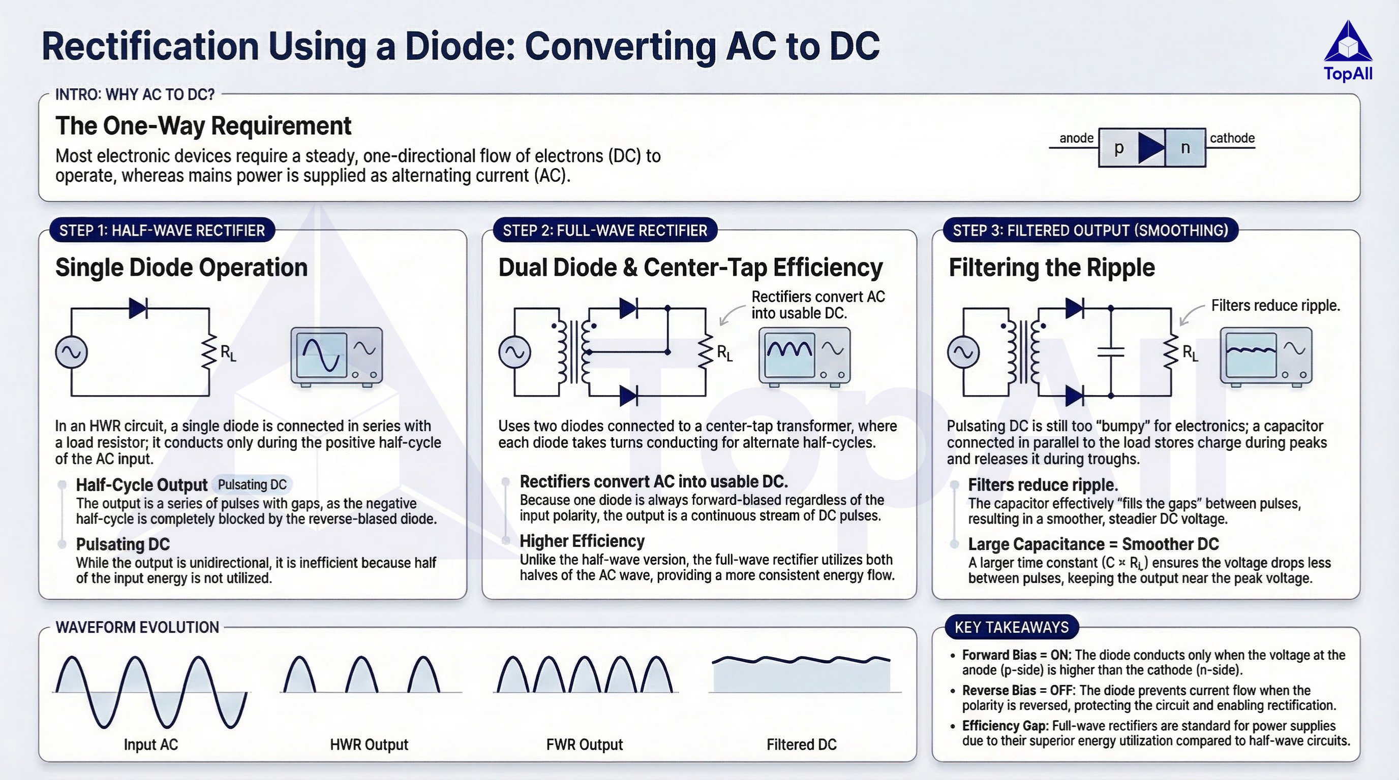
Learn rectifier applications with circuits & MCQs.
NEET UG · Mind map
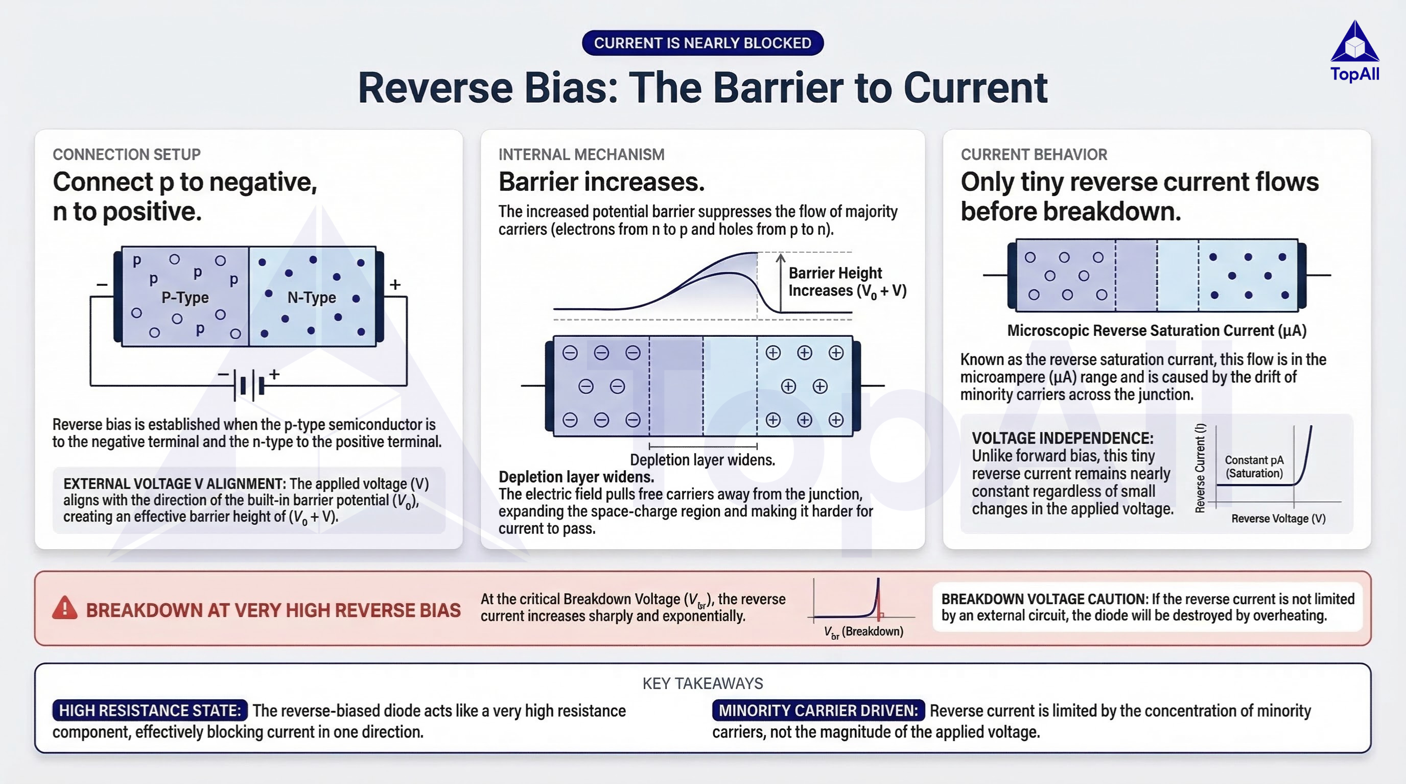
Master reverse bias concepts with examples & MCQs.
NEET UG · Mind map
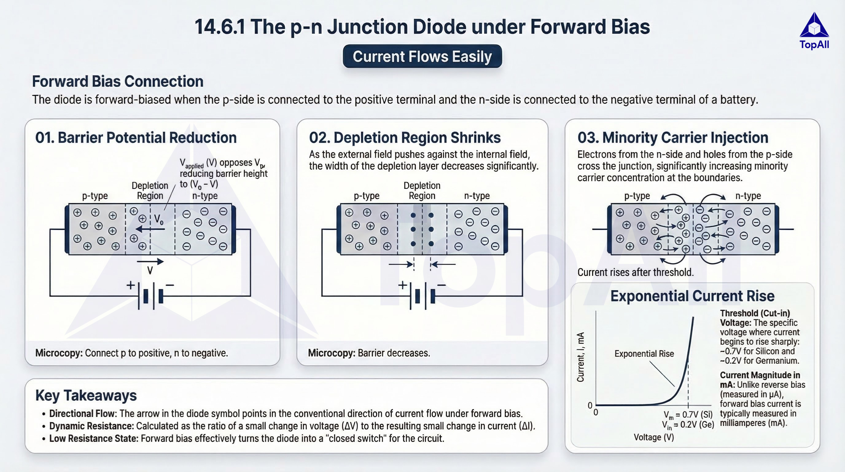
Learn forward bias in PN junction with diagrams & MCQs.
Explain junction charges and bias, test diode states and separate mean from RMS rectifier output.
For NEET UG Physics students: distinguish mobile carriers from fixed dopant ions, identify junction bias, test a diode model against its circuit and separate mean from RMS rectifier output.
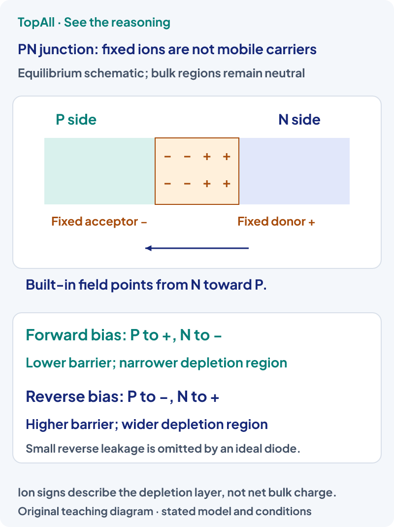
An n-type semiconductor has electrons as majority mobile carriers, while a p-type material has holes as majority carriers. The bulk can remain approximately electrically neutral because dopant-ion charge balances the carrier imbalance. Joining the materials forms a depleted region with fixed ionised acceptors on the P side and donors on the N side. Bias changes the barrier and carrier transport. A diode calculation must state whether the device is ideal, has a supplied constant forward drop or uses another I–V model.
At a supplied fixed temperature, take intrinsic carrier concentration and fully ionised donor density , with no acceptors. In the nondegenerate thermal-equilibrium model, and bulk charge neutrality gives . Since ND is much larger than ni, n≈ND and
Diffusion and recombination near the junction reduce mobile majority-carrier density and expose the fixed dopant-ion charge. At thermal equilibrium the opposing drift and diffusion contributions give zero net junction current, even though a built-in field exists. Forward bias reduces the barrier and depletion width; reverse bias increases them. A real reverse-biased diode can have minority-carrier leakage and, at sufficiently large reverse voltage, breakdown. Neither an ideal open reverse branch nor a constant 0.70 V forward drop describes every condition.
Consider a supplied 5.00 V DC source, series diode and 1.00 kΩ resistor to the source return. The source positive feeds the diode anode; its cathode feeds the resistor. Use a supplied constant forward drop 0.70 V when conducting. KVL gives . The positive current and forward orientation agree with the assumed state, and resistor voltage is 4.30 V. If the diode is reversed, a separate model that neglects leakage and stays below breakdown gives zero current; do not keep using the forward-drop equation. The 0.70 V here is a supplied approximation, not an exact universal silicon threshold.
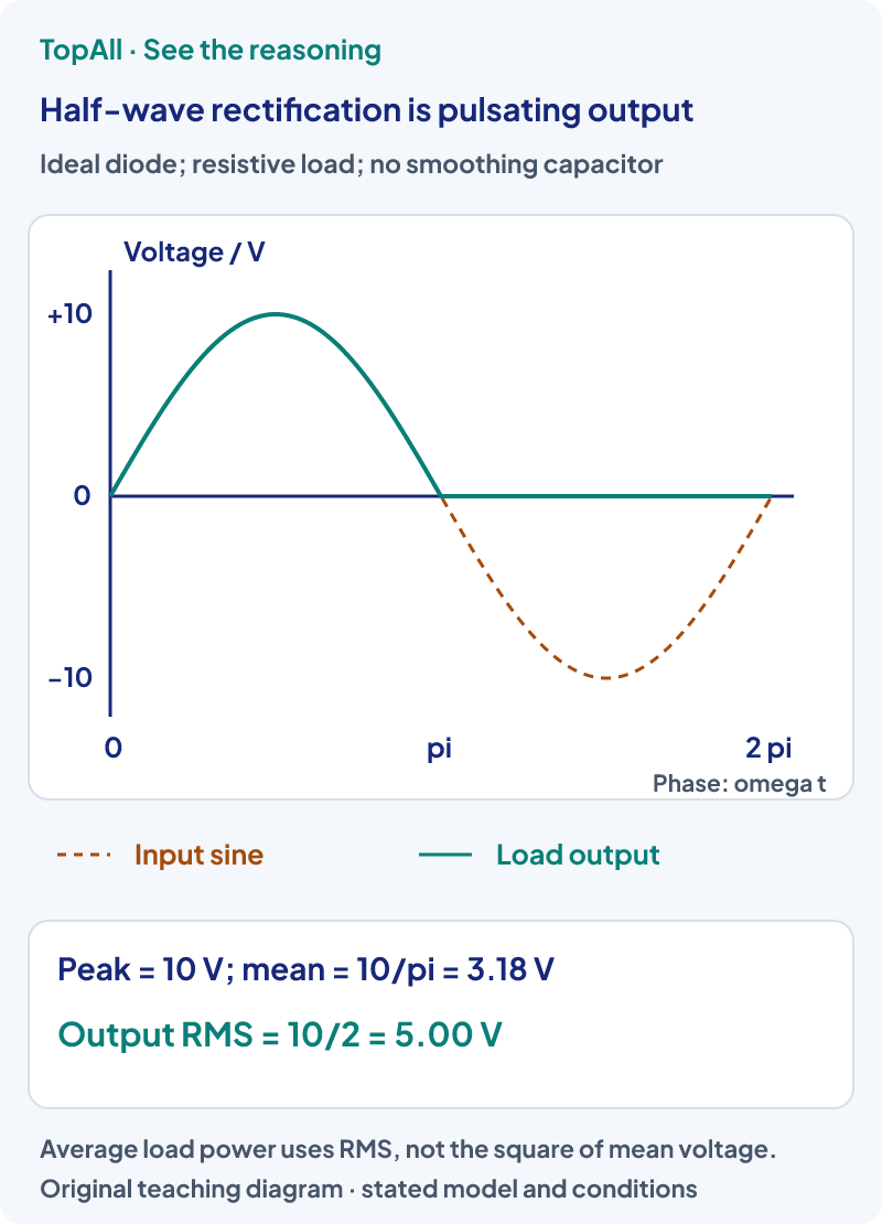
A rectifier makes a load waveform unidirectional in the chosen circuit. A half-wave ideal rectifier blocks one half-cycle, while a suitable full-wave arrangement redirects both halves. The resulting output can still vary strongly with time. A smoothing capacitor changes that waveform and requires assumptions about charging, discharge and load. Do not apply an unfiltered half-wave RMS or average formula to a capacitor-filtered output, or replace average power with a DC component alone when ripple remains.
For the plotted ideal half-wave sine take peak Vp=10.0 V and load R=1.00 kΩ. Over a full cycle, and . The load peak current is 10.0 mA and average power is
An intrinsic equilibrium material has equal electron and hole concentrations, but equal concentrations do not require equal electron and hole mobilities. An extrinsic sample is classified by the dopants and resulting carrier balance at its stated conditions. Raising temperature can change intrinsic generation and ionisation, so a room-temperature majority-carrier shortcut is not a universal statement for every temperature. A hole is a mobile missing-electron state in the valence system, not a proton moving through the crystal.
Do not label an n-type bulk block negatively charged or a p-type block positively charged merely from majority carriers. Depletion does not mean absence of fixed ions. Check terminal polarity and assumed state before applying a diode equation. Keep the ideal rectifier and supplied constant-drop models separate. Mean voltage, RMS voltage and average resistor power are different quantities; a pulsating output is not automatically smooth DC.
In the same anode-fed series circuit, replace the source by 0.50 V and retain the supplied 0.70 V constant-drop model, with reverse leakage omitted. Does the expression (0.50−0.70)/R mean a small reverse current flows through a forward-conducting diode?
No. The negative result contradicts the assumed forward-conducting state. In this piecewise approximation the diode is off and current is zero. A real diode has a smooth I–V characteristic, so the conclusion is about the supplied constant-drop model rather than an exact physical turn-on discontinuity.
For the same ideal half-wave resistive-load circuit, double the input peak from 10 V to 20 V. How do output mean, RMS and load average power change? Does the output become smooth DC?
The mean doubles to 20/π≈6.37 V and RMS doubles to 10.0 V. For the unchanged 1.00 kΩ load, average power quadruples from 25.0 mW to 100 mW. The waveform remains pulsating because no filter or other smoothing element was added.
Draw the fixed depletion charges from memory, then test a diode conducting-state assumption. Recalculate one rectifier load power using RMS. Continue to NEET Communication Systems for signal and envelope models, or NEET Alternating Current for peak, RMS and average quantities.
Chapter practice opens the broad Semiconductor Devices pool.
Technical review: Codex (automated). Primary textbook and university teaching sources checked on 23 October 2026. Diagrams, worked examples and questions are original and use explicit models. The archived 2018 Communication Systems exemplar supports concepts; this existing chapter catalogue does not establish current exam inclusion. Human subject review is not claimed.
Before the next set, write the device or signal model and the requested quantity. After a mistake, explain which assumption or comparison failed, then redo the calculation without viewing its answer.